建党100周年,伏达献礼推出100W电荷泵快充芯片
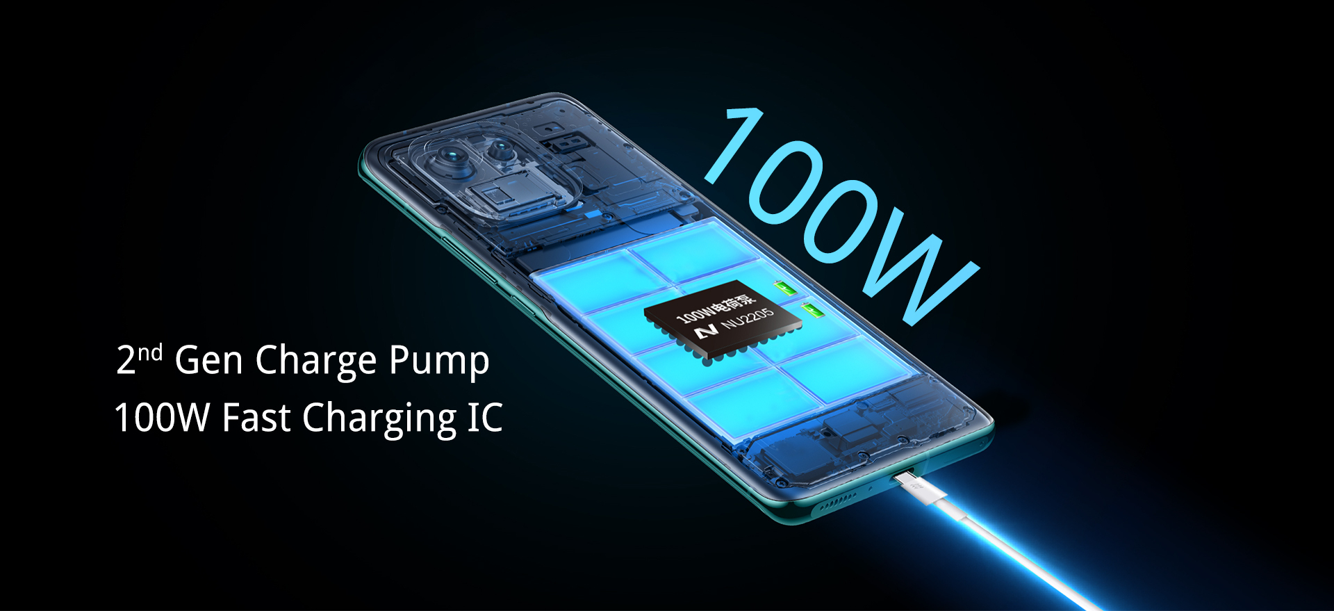
第二代电荷泵快充芯片
The 2nd Gen Charge Pump Fast Charging IC
第二代电荷泵快充芯片
The 2nd Gen Charge Pump Fast Charging IC
进入5G时代,智能手机耗电大幅增加,对快充的需求变得更加强烈。众所周知,全球第一代快充芯片由TI在2017年推出,国内芯片企业在两年后推出快充方案;第二代快充芯片发布于2020年11月,这一次,伏达仅用了半年就赶上了国际厂商,于2021年4月推出了100W快充芯片及方案。
In the 5G era, the power consumption of smartphones has increased significantly, and the demand for fast charging has become much stronger. As we all know, the world’s first generation of fast charging IC was launched by TI in 2017, which improved smartphone charging from 10W to 30W, even 40W. However, the battery anxiety keeps increasing with more and more powerful APPs and games on our smartphone. It keeps pushing for higher charging power up to 60W, or even 120W to shorten the charging time and cool the charging temperature. 1S battery charging limitation becomes the bottleneck to push for higher charging power. NU2205 brings an innovative 2S battery charging architecture, which changes the charging solution fundamentally to meet the increased charging power.
NU2205也是目前国内单芯片充电功率最高的电荷泵芯片,打破了国外芯片厂商在双电芯有线快充行业的垄断,伏达成为国内唯一能提供100W成熟快充方案的半导体公司,攻占快充功率制高点。
NU2205 is also the charge pump chip with the highest single-chip charging power in China, breaking the monopoly of foreign chip manufacturers in the wired fast charging industry. NuVolta is the only domestic semiconductor company that can provide a 100W mature fast charging solution, taking the commanding heights of fast charging power.
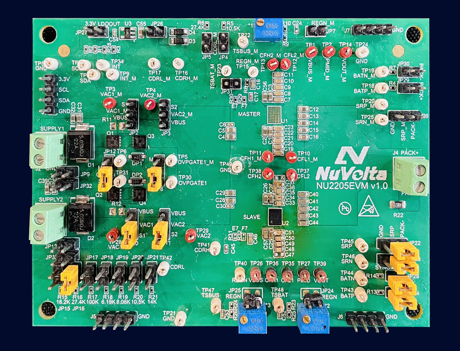
图1. NU2205 EVM
随着NU2205的推出,伏达将为手机客户提供高达200W的快充方案。
With the launch of NU2205, NuVolta will provide mobile phone customers with a fast-charging solution of up to 200W.
电荷泵快充芯片NU2205的性能优势
Performance Advantages of Charge Pump IC NU2205
NU2205利用创新的双电芯架构,在大于60W功率等级上,带来了全方位的优势。我们将从效率、温升及电流比对进行实验论证。
NU2205 utilizes an innovative 2S battery architecture to bring all-round advantages in power levels greater than 60W. The following are the experimental results of efficiency, temperature rise and current.
高效率
Higher Efficiency
高效率是快充应用里最关键的指标,NU2205不仅通过内部创新的结构提高了工作效率,同时也可以通过可调节的工作频率来调整效率。在4:2的工作模式下,最高效率可以达到98%,在10V适配器输入下,2:2模式2节电池充电效率最高可达99.2%。
High efficiency is the most critical parameter in fast charging applications. The NU2205 not only improves the work efficiency through the innovative internal structure, but can adjust the efficiency through the operating frequency. In the 4:2 mode, the highest efficiency can reach 98%. Under the 10V ACDC adapter input, the charging efficiency of 2S battery in the 2:2 mode can reach up to 99.2%.
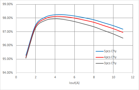
图2. 伏达NU2205充电效率曲线
Figure 2. NuVolta NU2205 charging efficiency curve
多模式
Multi-mode
NU2205除了4:2的双电芯电荷泵模式之外,还支持2:2的双电芯直充模式。在2:2直充模式,充电的效率高达99.2%。在高功率充电发热持续增加的应用环境里,提供了脉冲切换4:2和2:2两种模式降低系统的发热的可能。由于设计的创新性,NU2205还能同时支持2:1和1:1的单电芯快充模式。
In addition to the 4:2 2S battery charge pump mode, NU2205 also supports 2:2 2S battery direct charging mode. In the 2:2 direct charging mode, the charging efficiency is as high as 99.2%. In high power charging application, it provides the possibility of pulse switching between 4:2 and 2:2 modes to reduce the system’s heat. Due to the innovative design, NU2205 can also support both 2:1 and 1:1 1S battery fast charging modes.
温升测试图
Temperature Rise Test Chart
25°C环温条件下,16V输入时,2节电池在10A和20A大电流下充电,温升分别对应44.9°C/46.8°C。
At the conditions of 25°C ambient temperature and 16V input, when 2S batteries are charged at 10A and 20A current, the temperature rise is 44.9°C/46.8°C respectively shown as follows.
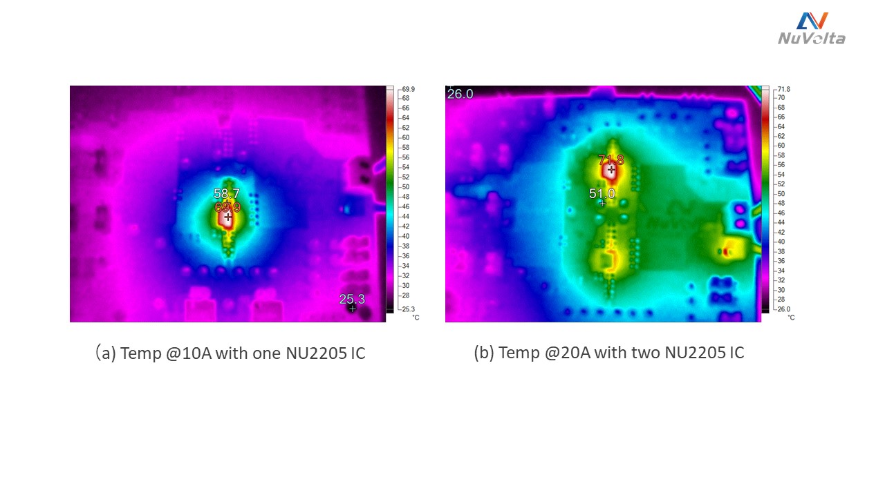
Figure 3. Temperature rise test under charging current
一颗NU2205实现10A充电
One NU2205 IC Achieves 10A Charging
如下图所示,用电子负载模拟电池快充过程,单颗NU2205芯片的EVM板,稳定输出10A电流。
As shown below, the electronic load is used to simulate the fast-charging process of the battery. The EVM board of a single NU2205 can output 10A current stably.
两颗NU2205并联实现20A充电
Two NU2205 ICs in Parallel to Achieve 20A Charging
如下图所示,用电子负载模拟电池快充过程,两颗NU2205芯片的EVM板,稳定输出20A电流。
As shown in the figure below, an electronic load is used to simulate the fast charging process of a battery. Two EVM boards with NU2205 can output a stable current of 20A.
双电芯架构的优势
Advantages of 2S Battery Architecture
NU2205采用伏达的双电芯4:2电荷泵快充架构,其单芯片最高功率支持100W。那么为什么要采用双电芯的架构呢?它有什么优势呢?
NU2205 adopts NuVolta’s 2S battery 4:2 charge pump fast charging architecture, and it supports charging power up to 100W with single chip. What are the advantages of 2S battery charging?
3.1 双电芯架构的突破性
The Breakthrough of 2S Battery Architecture
从2014年OPPO推出第一代电压大电流快充(VOOC)开始,到2017年单节电池电荷泵方案的商用,快充在单节电池分别突破了40W, 50W和60W。充入单节电池的电流也从开始的5A,增大到12A。这意味电芯内部的阻抗即使只有5mΩ,电芯的功率损耗也超过了0.7W。超大的电流和超高的发热对电池保护板的设计和电芯内部阻抗带来了巨大的挑战。
Along with OPPO launched the first generation of low-voltage high-current fast charging (VOOC) in 2014, the fast charging solution has dramatically changed the way of battery charging in smartphones. In 2017, the 1S battery charge pump solution was commercially available by TI, and the charging power exceeded 40W, 50W and 60W in 1S battery charging. The current charges into the 1S battery have also increased from the initial 5A to 12A. That means when the battery’s internal resistance is only 5mΩ, the power loss of battery exceeds 0.7W. The higher current brings more heat that induces huge challenges to the design of the battery protection board and the internal resistance of the battery cell.
以电池保护MOSFET为例,为了满足快充大电流的应用,MOSFET的阻抗已经从5mΩ降低到了1.1mΩ。这意味着电池保护MOSFET性能已接近了器件极限,使得单节电池功率的提升要付出更高的代价。
Taking battery protection MOSFET as an example. In order to meet the application of fast charging and high current, the resistance of MOSFET has been reduced from 5mΩ to 1.1mΩ. It means the battery protection MOSFET performance has approached the device limit. Therefore, the 1S battery fast charging encounters the charging power limitation.
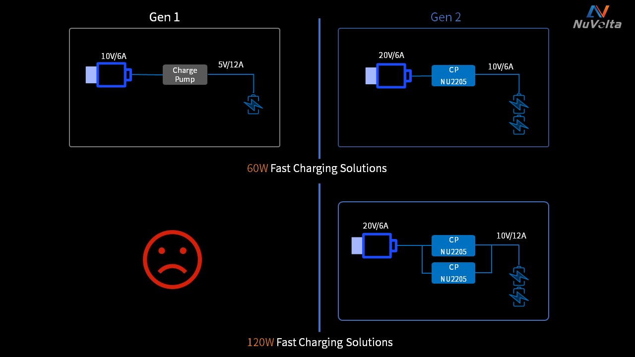
双电芯快充方案在充电输出端把电池电压提高一倍,在同样的充电功率下进入电芯的电流减小一半,电芯的发热减小到25%。同样在60W的充电功率档,进入电芯的电流降到6A,保持电池包5mΩ内阻的情况下,电芯的功率损耗显著降低到180mW;在保持同样电芯电流的情况下,双电芯快充可以突破单电芯功率限制达到120W,甚至是200W。
The 2S battery fast charging solution doubles the battery voltage at the charging output terminal, reduces the current into the battery by half at the same charging power, and reduces the battery’s heat to 25%. In the same 60W charging power level, the current to the battery drops to 6A. When the battery pack’s internal resistance keeps 5mΩ, the power loss of the battery is significantly reduced to 180mW; When the current to battery keep 12A, 2S battery fast charging can break through the charging power limit to 120W, or even 200W.
第二代电荷泵快充芯片——NU2205采用4:2电荷泵架构,这种架构和集成FET进行了优化,可实现50%的占空比。使电缆电流成为传输到电池电流的一半,从而减少了充电电缆的损耗并限制了应用中的温升。 双相架构降低了输入电容要求,同时降低了输出电压纹波。
The second-generation charge pump fast charge IC - NU2205 adopts 4:2 charge pump architecture. This architecture and integrated FET have been optimized to achieve a 50% duty cycle. The architecture lowers down the current of USB cable to half of charging current to battery, reducing the loss of the charging cable and limiting the temperature rise in the application. The two-phase architecture lowers down the input capacitance requirements while improving the output voltage ripple.
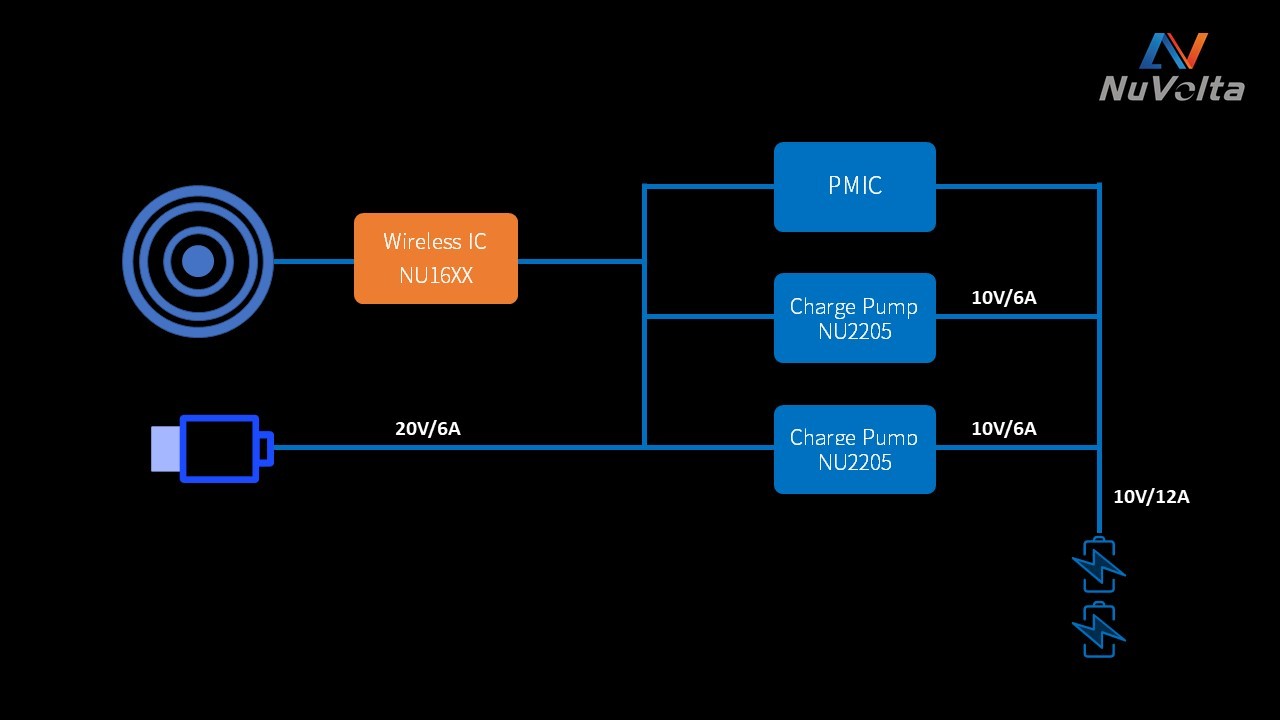
Figure 4. Advantages of 2S battery architecture
如上图所示,将输入端20V电压降低50%传到电池端,然而电池端获得了2倍输入端电流12A的充电电流,输入端电流被限定在6A内的同时,既实现了高功率传输,又无需升级充电线缆,凸显了双电芯架构的优势。
As shown in Figure 4, the input 20V voltage is reduced by 50% at battery packs side and the charging current of battery is increased to 12A current, which is twice of the input current. In light of the current double structure, the input current is limited to 6A that can realize high power transmission while no need to upgrade the charging cable, demonstrating advantages of the 2S battery architecture.
更重要的是,NU2205可支持多芯片并联工作,如果将两颗NU2205并联,可实现充电功率120W的突破,一举斩获业界充电功率最高的殊荣。如果将三颗NU2205并联,那么充电功率将突破200W,而这种技术是单电芯方案无可比拟的。
Furthermore, NU2205 supports charging parallelly. When two NU2205 ICs are used in parallel, the charge pump ICs will output 120W power.
When three NU2205 ICs are in parallel, the charging power exceeds 200W.
全面的保护机制,多达34重
Completed Safety Protections
在高功率充电应用中,效率和发热是大家最关注的指标。然而,在充电系统中,除了效率,最重要的是充电安全。NU2205集成多达34重全面保护,全方位保护输入与输出电压电流、电池电压电流及温度等,有效保护系统,防止异常情况对电池和系统造成损坏。我们比你更在乎充电安全。
In high-power charging applications, efficiency and heat are the most important considerations. However, in a charging system, besides efficiency, the most important consideration is charging safety. NU2205 integrates up to 34 levels of safety protections, such as protections of input and output voltage and current, battery voltage and current, and temperature, etc. That protects the system and prevents abnormal conditions damaging the battery and system. We care more about charging safety than you.
完整的无线充电与有线快充方案
Offers both Wireless Charging and Wired Fast Charging Solutions
在与国际厂商的竞争中,伏达半导体冲在前线,率先打破国外芯片厂商在有线快充行业的垄断,攻占了快充功率制高点,扭转了核心技术被钳制的局面。伏达的竞争优势还体现在已有的领先的无线快充技术。新推出的100W快充方案与伏达业界功率最高的无线快充方案相得益彰,形成完整无线加有线的快充方案。毫无疑问,伏达半导体成为唯一一家能同时提供无线充电与有线快充方案的半导体公司。
NuVolta’s competitive advantage is also reflected in the existing leading wireless fast charging technology. Together with the world-leading wireless fast charging solution, the newly launched 100W fast charging solution enables NuVolta to be a unique high-performance power semiconductor company with competed wireless and wired fast charging solution.
总结
Summary
伏达推出第二代电荷泵快充芯片,旨在帮助智能手机客户解决快充过程中的功耗过高、升温过快等问题,并将充电效率做到业界最优。凭借过硬的产品品质,伏达已经与多个品牌客户合作了快充项目。随着充电功率的提高与效率的不断提升,伏达的快充系列产品将帮助客户,极大改善用户的充电体验。
NuVolta launched the second-generation charge pump fast charging IC, which aims to empower smartphone customers to solve the problems of high-power consumption and heating during fast charging, and achieve the best charging efficiency in the industry. With excellent product quality, NuVolta has cooperated with many brand customers in fast charging projects. With the improvement of charging power and efficiency, NuVolta fast charging series products will help customers and greatly improve the charging experience of users.
关于伏达半导体
About NuVolta Technologies
伏达半导体(NuVolta Technologies)成立于2014年,专注于电源管理芯片及方案的研发及创新,是业界唯一同时提供成熟的无线充电与有线快充方案的半导体公司。伏达通过对工艺、设计、封装及电源系统构架的不断创新,持续为客户输出高性能、高效率、高可靠性的芯片产品及整体解决方案。我们的产品涵盖无线充电接收和发射芯片、有线快充芯片、显示电源芯片与汽车电源管理芯片等,助力客户持续拓展消费类电子、汽车电子、工业医疗等市场。伏达致力于让更多的用户感受科技创新所带来的便捷与乐趣。欲了解更多信息,请浏览伏达半导体官网,或发邮件至sales@nuvoltatech.com咨询相关业务。
Founded in 2014 in Silicon Valley, NuVolta Technologies is the industry’s leading supplier of ICs and solutions. We are committed to providing high-performance power management ICs and power system solutions for Consumer Electronics, Automotive, Industrial and Healthcare. Our products cover wireless charging receiving and transmitting ICs, fast charging ICs, display power ICs and protection ICs. NuVolta has become a core supplier of international mainstream smartphone brands and few mobile accessory manufacturers. Meanwhile, our one-stop power management solution has become primary choice of internationally renowned consumer electronics brands. For more information, please visit , or send an email to .
进入5G时代,智能手机耗电大幅增加,对快充的需求变得更加强烈。众所周知,全球第一代快充芯片由TI在2017年推出,国内芯片企业在两年后推出快充方案;第二代快充芯片发布于2020年11月,这一次,伏达仅用了半年就赶上了国际厂商,于2021年4月推出了100W快充芯片及方案。
In the 5G era, the power consumption of smartphones has increased significantly, and the demand for fast charging has become much stronger. As we all know, the world’s first generation of fast charging IC was launched by TI in 2017, which improved smartphone charging from 10W to 30W, even 40W. However, the battery anxiety keeps increasing with more and more powerful APPs and games on our smartphone. It keeps pushing for higher charging power up to 60W, or even 120W to shorten the charging time and cool the charging temperature. 1S battery charging limitation becomes the bottleneck to push for higher charging power. NU2205 brings an innovative 2S battery charging architecture, which changes the charging solution fundamentally to meet the increased charging power.
NU2205也是目前国内单芯片充电功率最高的电荷泵芯片,打破了国外芯片厂商在双电芯有线快充行业的垄断,伏达成为国内唯一能提供100W成熟快充方案的半导体公司,攻占快充功率制高点。
NU2205 is also the charge pump chip with the highest single-chip charging power in China, breaking the monopoly of foreign chip manufacturers in the wired fast charging industry. NuVolta is the only domestic semiconductor company that can provide a 100W mature fast charging solution, taking the commanding heights of fast charging power.
图1. NU2205 EVM
随着NU2205的推出,伏达将为手机客户提供高达200W的快充方案。
With the launch of NU2205, NuVolta will provide mobile phone customers with a fast-charging solution of up to 200W.
电荷泵快充芯片NU2205的性能优势
Performance Advantages of Charge Pump IC NU2205
NU2205利用创新的双电芯架构,在大于60W功率等级上,带来了全方位的优势。我们将从效率、温升及电流比对进行实验论证。
NU2205 utilizes an innovative 2S battery architecture to bring all-round advantages in power levels greater than 60W. The following are the experimental results of efficiency, temperature rise and current.
高效率
Higher Efficiency
高效率是快充应用里最关键的指标,NU2205不仅通过内部创新的结构提高了工作效率,同时也可以通过可调节的工作频率来调整效率。在4:2的工作模式下,最高效率可以达到98%,在10V适配器输入下,2:2模式2节电池充电效率最高可达99.2%。
High efficiency is the most critical parameter in fast charging applications. The NU2205 not only improves the work efficiency through the innovative internal structure, but can adjust the efficiency through the operating frequency. In the 4:2 mode, the highest efficiency can reach 98%. Under the 10V ACDC adapter input, the charging efficiency of 2S battery in the 2:2 mode can reach up to 99.2%.
图2. 伏达NU2205充电效率曲线
Figure 2. NuVolta NU2205 charging efficiency curve
多模式
Multi-mode
NU2205除了4:2的双电芯电荷泵模式之外,还支持2:2的双电芯直充模式。在2:2直充模式,充电的效率高达99.2%。在高功率充电发热持续增加的应用环境里,提供了脉冲切换4:2和2:2两种模式降低系统的发热的可能。由于设计的创新性,NU2205还能同时支持2:1和1:1的单电芯快充模式。
In addition to the 4:2 2S battery charge pump mode, NU2205 also supports 2:2 2S battery direct charging mode. In the 2:2 direct charging mode, the charging efficiency is as high as 99.2%. In high power charging application, it provides the possibility of pulse switching between 4:2 and 2:2 modes to reduce the system’s heat. Due to the innovative design, NU2205 can also support both 2:1 and 1:1 1S battery fast charging modes.
温升测试图
Temperature Rise Test Chart
25°C环温条件下,16V输入时,2节电池在10A和20A大电流下充电,温升分别对应44.9°C/46.8°C。
At the conditions of 25°C ambient temperature and 16V input, when 2S batteries are charged at 10A and 20A current, the temperature rise is 44.9°C/46.8°C respectively shown as follows.
Figure 3. Temperature rise test under charging current
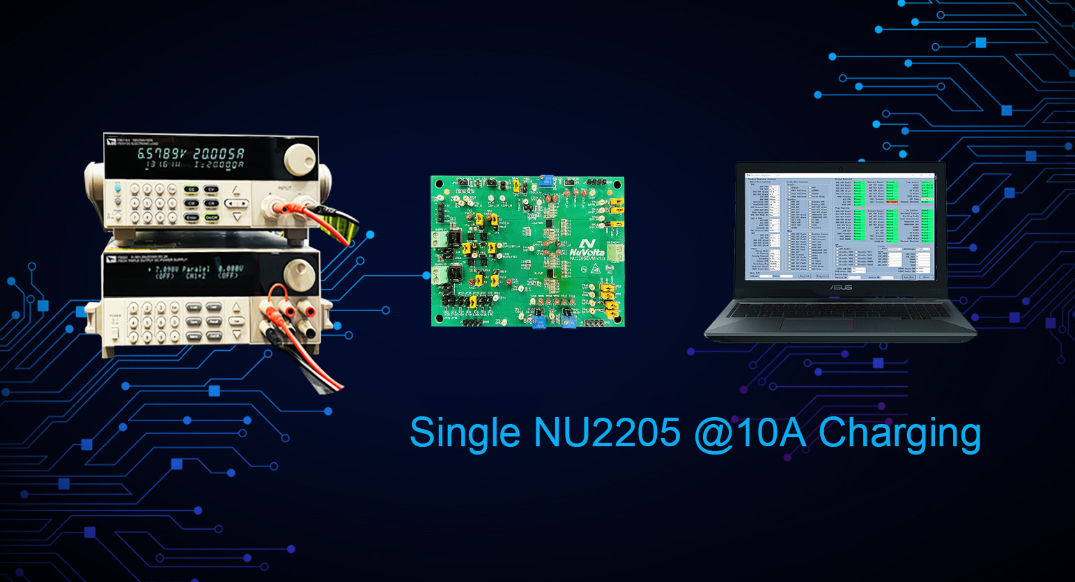
一颗NU2205实现10A充电
One NU2205 IC Achieves 10A Charging
如下图所示,用电子负载模拟电池快充过程,单颗NU2205芯片的EVM板,稳定输出10A电流。
As shown below, the electronic load is used to simulate the fast-charging process of the battery. The EVM board of a single NU2205 can output 10A current stably.
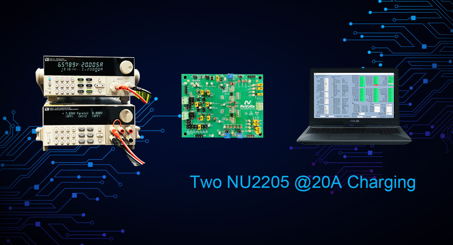
两颗NU2205并联实现20A充电
Two NU2205 ICs in Parallel to Achieve 20A Charging
如下图所示,用电子负载模拟电池快充过程,两颗NU2205芯片的EVM板,稳定输出20A电流。
As shown in the figure below, an electronic load is used to simulate the fast charging process of a battery. Two EVM boards with NU2205 can output a stable current of 20A.
双电芯架构的优势
Advantages of 2S Battery Architecture
NU2205采用伏达的双电芯4:2电荷泵快充架构,其单芯片最高功率支持100W。那么为什么要采用双电芯的架构呢?它有什么优势呢?
NU2205 adopts NuVolta’s 2S battery 4:2 charge pump fast charging architecture, and it supports charging power up to 100W with single chip. What are the advantages of 2S battery charging?
3.1 双电芯架构的突破性
The Breakthrough of 2S Battery Architecture
从2014年OPPO推出第一代电压大电流快充(VOOC)开始,到2017年单节电池电荷泵方案的商用,快充在单节电池分别突破了40W, 50W和60W。充入单节电池的电流也从开始的5A,增大到12A。这意味电芯内部的阻抗即使只有5mΩ,电芯的功率损耗也超过了0.7W。超大的电流和超高的发热对电池保护板的设计和电芯内部阻抗带来了巨大的挑战。
Along with OPPO launched the first generation of low-voltage high-current fast charging (VOOC) in 2014, the fast charging solution has dramatically changed the way of battery charging in smartphones. In 2017, the 1S battery charge pump solution was commercially available by TI, and the charging power exceeded 40W, 50W and 60W in 1S battery charging. The current charges into the 1S battery have also increased from the initial 5A to 12A. That means when the battery’s internal resistance is only 5mΩ, the power loss of battery exceeds 0.7W. The higher current brings more heat that induces huge challenges to the design of the battery protection board and the internal resistance of the battery cell.
以电池保护MOSFET为例,为了满足快充大电流的应用,MOSFET的阻抗已经从5mΩ降低到了1.1mΩ。这意味着电池保护MOSFET性能已接近了器件极限,使得单节电池功率的提升要付出更高的代价。
Taking battery protection MOSFET as an example. In order to meet the application of fast charging and high current, the resistance of MOSFET has been reduced from 5mΩ to 1.1mΩ. It means the battery protection MOSFET performance has approached the device limit. Therefore, the 1S battery fast charging encounters the charging power limitation.
双电芯快充方案在充电输出端把电池电压提高一倍,在同样的充电功率下进入电芯的电流减小一半,电芯的发热减小到25%。同样在60W的充电功率档,进入电芯的电流降到6A,保持电池包5mΩ内阻的情况下,电芯的功率损耗显著降低到180mW;在保持同样电芯电流的情况下,双电芯快充可以突破单电芯功率限制达到120W,甚至是200W。
The 2S battery fast charging solution doubles the battery voltage at the charging output terminal, reduces the current into the battery by half at the same charging power, and reduces the battery’s heat to 25%. In the same 60W charging power level, the current to the battery drops to 6A. When the battery pack’s internal resistance keeps 5mΩ, the power loss of the battery is significantly reduced to 180mW; When the current to battery keep 12A, 2S battery fast charging can break through the charging power limit to 120W, or even 200W.
第二代电荷泵快充芯片——NU2205采用4:2电荷泵架构,这种架构和集成FET进行了优化,可实现50%的占空比。使电缆电流成为传输到电池电流的一半,从而减少了充电电缆的损耗并限制了应用中的温升。 双相架构降低了输入电容要求,同时降低了输出电压纹波。
The second-generation charge pump fast charge IC - NU2205 adopts 4:2 charge pump architecture. This architecture and integrated FET have been optimized to achieve a 50% duty cycle. The architecture lowers down the current of USB cable to half of charging current to battery, reducing the loss of the charging cable and limiting the temperature rise in the application. The two-phase architecture lowers down the input capacitance requirements while improving the output voltage ripple.
Figure 4. Advantages of 2S battery architecture
如上图所示,将输入端20V电压降低50%传到电池端,然而电池端获得了2倍输入端电流12A的充电电流,输入端电流被限定在6A内的同时,既实现了高功率传输,又无需升级充电线缆,凸显了双电芯架构的优势。
As shown in Figure 4, the input 20V voltage is reduced by 50% at battery packs side and the charging current of battery is increased to 12A current, which is twice of the input current. In light of the current double structure, the input current is limited to 6A that can realize high power transmission while no need to upgrade the charging cable, demonstrating advantages of the 2S battery architecture.
更重要的是,NU2205可支持多芯片并联工作,如果将两颗NU2205并联,可实现充电功率120W的突破,一举斩获业界充电功率最高的殊荣。如果将三颗NU2205并联,那么充电功率将突破200W,而这种技术是单电芯方案无可比拟的。
Furthermore, NU2205 supports charging parallelly. When two NU2205 ICs are used in parallel, the charge pump ICs will output 120W power.
When three NU2205 ICs are in parallel, the charging power exceeds 200W.
全面的保护机制,多达34重
Completed Safety Protections
在高功率充电应用中,效率和发热是大家最关注的指标。然而,在充电系统中,除了效率,最重要的是充电安全。NU2205集成多达34重全面保护,全方位保护输入与输出电压电流、电池电压电流及温度等,有效保护系统,防止异常情况对电池和系统造成损坏。我们比你更在乎充电安全。
In high-power charging applications, efficiency and heat are the most important considerations. However, in a charging system, besides efficiency, the most important consideration is charging safety. NU2205 integrates up to 34 levels of safety protections, such as protections of input and output voltage and current, battery voltage and current, and temperature, etc. That protects the system and prevents abnormal conditions damaging the battery and system. We care more about charging safety than you.
完整的无线充电与有线快充方案
Offers both Wireless Charging and Wired Fast Charging Solutions
在与国际厂商的竞争中,伏达半导体冲在前线,率先打破国外芯片厂商在有线快充行业的垄断,攻占了快充功率制高点,扭转了核心技术被钳制的局面。伏达的竞争优势还体现在已有的领先的无线快充技术。新推出的100W快充方案与伏达业界功率最高的无线快充方案相得益彰,形成完整无线加有线的快充方案。毫无疑问,伏达半导体成为唯一一家能同时提供无线充电与有线快充方案的半导体公司。
NuVolta’s competitive advantage is also reflected in the existing leading wireless fast charging technology. Together with the world-leading wireless fast charging solution, the newly launched 100W fast charging solution enables NuVolta to be a unique high-performance power semiconductor company with competed wireless and wired fast charging solution.
总结
Summary
伏达推出第二代电荷泵快充芯片,旨在帮助智能手机客户解决快充过程中的功耗过高、升温过快等问题,并将充电效率做到业界最优。凭借过硬的产品品质,伏达已经与多个品牌客户合作了快充项目。随着充电功率的提高与效率的不断提升,伏达的快充系列产品将帮助客户,极大改善用户的充电体验。
NuVolta launched the second-generation charge pump fast charging IC, which aims to empower smartphone customers to solve the problems of high-power consumption and heating during fast charging, and achieve the best charging efficiency in the industry. With excellent product quality, NuVolta has cooperated with many brand customers in fast charging projects. With the improvement of charging power and efficiency, NuVolta fast charging series products will help customers and greatly improve the charging experience of users.
关于伏达半导体
About NuVolta Technologies
伏达半导体(NuVolta Technologies)成立于2014年,专注于电源管理芯片及方案的研发及创新,是业界唯一同时提供成熟的无线充电与有线快充方案的半导体公司。伏达通过对工艺、设计、封装及电源系统构架的不断创新,持续为客户输出高性能、高效率、高可靠性的芯片产品及整体解决方案。我们的产品涵盖无线充电接收和发射芯片、有线快充芯片、显示电源芯片与汽车电源管理芯片等,助力客户持续拓展消费类电子、汽车电子、工业医疗等市场。伏达致力于让更多的用户感受科技创新所带来的便捷与乐趣。欲了解更多信息,请浏览伏达半导体官网,或发邮件至sales@nuvoltatech.com咨询相关业务。
Founded in 2014 in Silicon Valley, NuVolta Technologies is the industry’s leading supplier of ICs and solutions. We are committed to providing high-performance power management ICs and power system solutions for Consumer Electronics, Automotive, Industrial and Healthcare. Our products cover wireless charging receiving and transmitting ICs, fast charging ICs, display power ICs and protection ICs. NuVolta has become a core supplier of international mainstream smartphone brands and few mobile accessory manufacturers. Meanwhile, our one-stop power management solution has become primary choice of internationally renowned consumer electronics brands. For more information, please visit , or send an email to .
本站所有转载文章系出于传递更多信息之目的,且明确注明来源,不希望被转载的媒体或个人可与我们联系,我们将立即进行删除处理。